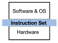
The success of CMOS* as the most widely used semiconductor* technology is the result of continuously shrinking the key feature size parameters (channel length L_min, transistor width w, and oxide thickness t_ox) of the MOSFET transistors.
Moore’s Law: The number of transistors per chip will continue to double every 18 – 24 months (two years). Note doubling the number of transistors per area implies a shrinking of both L_min and the transistor width w by .
CMOS power dissipation density, i.e. power per area, is proportional to the number of transistor devices per area, the switched gate-substrate capacity per device, the device operation frequency, and the square of the supply voltage.
Reducing L_min, w, and t_ox of transistors in the next CMOS generation by a factor of lowers the gate-substrate capacity C by too. Thus, implementing the same circuitry (N, f = const.) lowers power dissipation by roughly 30% when the supply voltage remains constant. However, as the number of devices per area increases by a factor of 2, the chip power dissipation density should increase by a factor of , or 40% per CMOS generation.
There are various reasons why CMOS has become dominant. First, the growth of silicon oxide (SiO2) on the silicon surface is controllable. The fabrication of MOS transistors is highly integratable and easy to design. A second benefit of CMOS circuits results from their electrical behavior. Due to the use of complementary transistors, they offer low power dissipation, high noise immunity, and easy cascadibility of logic gates.
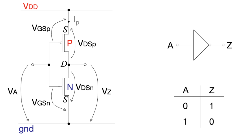
The source is defined as the source of carriers, so the source of nMOS is on lower potential; the source of pMOS is on higher potential. The gate-source voltage V_gs of nMOS needs to be positive to generate a conductive channel, whereas V_gs needs to be negative for pMOS.
The propagation delay time of CMOS circuits is . In order to obtain higher speed circuits, capacitive load Cload, oxide thickness tox, channel length Lp, and absolute threshold voltages |Vtp| have to be decreased, whereas carrier mobility μp, channel width Wp, relative oxide dielectric εox, and supply voltage Vdd have to be increased. This is valid for minimizing the delay time of a circuit only. If we want to optimize area and power consumption at the same time, there are conflicts.
Dynamic power* is mainly related to the functionality of the circuit, it is signal-edge-dependent. It consists of a capacitive part and a short-circuit part. Static power is related to parasitic effects, like sub-threshold current, leakage current, and gate tunneling current. It is signal-level-dependent.
Dynamic Capacitive Power: With the switching activity of α_01, the capacitive power dissipation of CMOS is .
Dynamic Short Circuit Power: Under the following assumption, the short circuit time is .
Static Sub-threshold Currents: An ideal MOS transistor should be completely switched off as long as the gate-source voltage is below the threshold voltage level. But in a real transistor, there will be sub-threshold currents.
Static Diode Leakage / Gate Current: The gate oxide of a MOS transistor is not a perfect isolator. There is some marginal resistance, some ionic conduction related to trapped ions inside the oxide, and some tunneling through the oxide.
If everything is done right, there will never be a conducting path between Vdd and GND.
All logic functions can be expressed using NAND and NOR
semiconductor
Semiconductors are materials that have an electrical conductivity that is intermediate between that of a conductor and an insulator. They are generally made from elements such as silicon or germanium, and their conductivity can be controlled by adding impurities (doping) to the material.
CMOS
CMOS, or Complementary Metal-Oxide-Semiconductor, is a type of technology used to create semiconductor devices, such as transistors. By applying a voltage to the gate of the transistor, it is possible to control the flow of current between source and drain, which allows the transistor to function as an amplifier, switch, etc.
Dynamic power dissipation
Dynamic power dissipation is the power consumed by a CMOS circuit when it is actively switching, or changing states. This power is associated with the movement of charges within the circuit and is proportional to the switching frequency of the circuit.
In a CMOS (complementary metal-oxide-semiconductor) circuit, dynamic capacitive power dissipation is caused by the charging and discharging of the parasitic capacitances present within the circuit. It is proportional to the switching frequency of the circuit and the total capacitance of the circuit. As a result, it can be a significant contributor to the overall power consumption of a high-speed CMOS circuit.
Static power dissipation
Static power dissipation is the power consumed by a CMOS circuit when it is not actively switching, or when it is in a static state. This power is associated with the leakage of current through the transistors in the circuit and is independent of the switching frequency.
2. SoC Logic Design Recap
As a consequence of DeMorgan’s rule, all logic functions can be expressed by combinations of either NAND or NOR gates. Furthermore, Boolean equations can be easily converted to static CMOS circuits.
In general, a generic model can be used to convert Boolean equations into static CMOS circuits. Each AND function generates serially connected nMOS transistors on a path from the output to GND, complemented by parallel connected pMOS transistors on a path from the output to VDD. Each OR function generates parallel nMOS, complemented by serial pMOS transistors, respectively. Finally, the output is always inverted, due to the switching properties of MOS transistors.
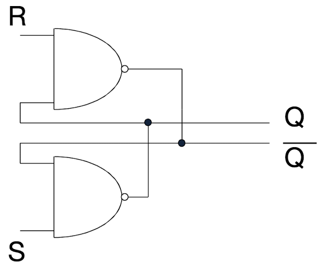
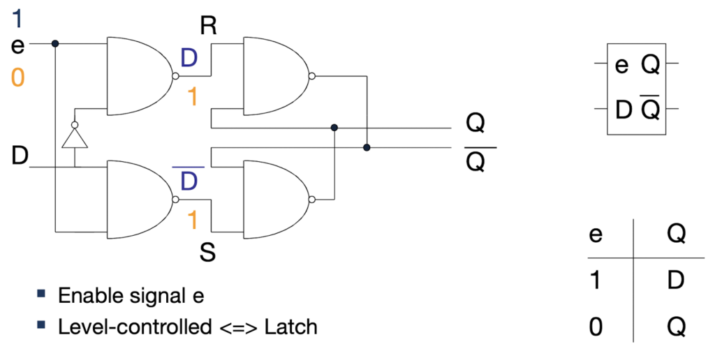
The basic CMOS storage element consists of a loop of two inverters. Connected together, they form a stable circuit, which can stick to either “1” or “0” at the corresponding nodes. The circuit has just outputs, but no inputs, in order to set a specific logic value, we need to open the loop. This can be done by substituting the inverters with NAND gates. A control input x is used to determine the functionality of the NAND gate: For x = 1, the NAND gate operates like an inverter. For x = 0, the output of the NAND gate switches to “1”, thus setting “1” into the loop.
In contrast to the level-controlled latch, a flip-flop is clock edge-controlled. A flip-flop consists of two serially connected latches, a Master and a Slave. A clock signal is used to control the enable inputs of both latches.
When the clock signal is “0”, e = 1 for the first latch, the value of input D is set into the Master latch. At the same time, the Slave latch is locked to the previous value of Q. When the clock signal switches to “1”, e = 1 for the second latch, the Slave latch is set to the current value of the Master latch. Any further change at the input D does not affect the Slave latch, as the Master latch is locked in this state.
Overall, the flip-flop is set to the current value of the input D at the positive clock edge, whereas for all other times, the output Q of the flip-flop is locked.
For each flip-flop, three characteristic parameters are specified: The setup-time t_setup, the hold time t_hold, and the clock-to-output delay t_c2q. The first two parameters t_setup and t_hold impose restrictions on the input signal of the flip- flop. The input signal D must be stable* for the setup-time before clock edge and for the hold-time after clock edge. This is required in order to guarantee correct setting of the flip-flop at the clock edge and to avoid metastability. The third parameter, t_c2q, specifies the delay after the clock edge until the valid data will be visible at the output.
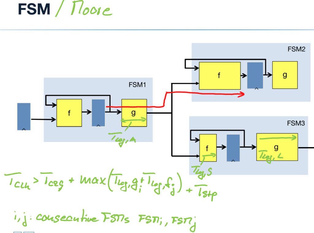
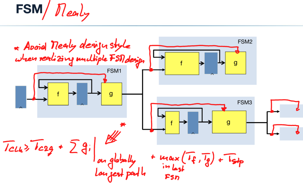
Finite State Machines (FSMs) consist of a register bank, input logic, output logic, and a feedback loop. The input logic f(x,u) combines primary inputs x with current-state vector u = [D_1 to D_n] to generate the next-state vector v = [Q_1 to Q_n]. The output logic g(x,u) or g(u) generate the output vector y. The clock signal switches the register bank from the current state to the next state.
Communicating FSMs are sequences of combinatorial logic and registers. The maximum clock frequency is limited by the propagation time through the combinatorial logic, the setup time, and the clock-to-output delay of the registers: .
The data input is latched (or captured) at the moment the clock edge occurs, which is typically the rising edge of the clock pulse. The flip-flop then holds the captured data in its internal memory until the next clock edge occurs, at which point the process repeats. It is important to ensure that the data input remains stable before and after the clock edge occurs in order to ensure the correct operation of the flip-flop.
3. SoC Paradigm*
Boolean Algebra enables a formal mathematical treatment of logic circuitry expressions and transformation/reduction into simpler expressions – the beginning of logic term minimization. At the beginning of the 90s, the trend resulted in more abstract building blocks in IC design.
To keep up with the Moore’s law further, the entire circuit can be represented as a SoC platform. SoC is an integrated system design paradigm where large portions of a chip are assembled from already existing function blocks maintained in so called Core or Macro Libraries. Examples of SoC function blocks are: Microprocessor cores (ARM, MIPS, PowerPC), em- bedded SRAM, on-chip busses (AMBA, CoreConnect, OCP), network interfaces (10/100 Ethernet, Gigabit Ethernet, SONET/SDH), system interfaces (PCI, Rapid I/O) and standard peripherals (UART, I2C, GPIO).
为什么不在多个微处理器上运行的软件中实现所有功能?为什么不在硬件中实现所有功能?——Computationa Density 和 Function Diversity 是选择最符合灵活性/性能要求的特定技术来实现SoC功能的主要动机。
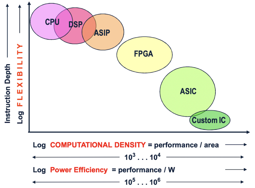
The most flexible alternative to implement a certain function is by means of a general purpose processor (CPU). The functionality of the CPU is solely determined by the instruction sequences of the program memory. On the other extreme of the flexibility dimension is custom IC or custom ASIC technology. Once you have designed and manufactured a certain function in custom IC technology, it’s rock solid and can’t be changed without re-design and re-manufacturing. However, when you compare the two implementations (CPU vs. custom IC) of one and the same function from a chip area and power consumption perspective, custom IC is by up to a factor 10’000 (in area) and 1’000’000 (in power) more efficient than CPU.
Computational density (CD) is defined as computations per unit area and time. Functional Diversity (FD) can either be interpreted as the number of instructions per compute element which is stored local to the compute unit, or as an empiric metric to express the flexibility of a specific implementation technique.
The range of hardware implementation techniques spans from standard software programmable microprocessor/DSP cores, to Application Specific Instruction Processors (ASIP), to Field Programmable Gate arrays (FPGA)*, to Application Specific Integrated Circuits (ASIC) and (full) custom IC.
The difference between Standard Cell and Macro Cell SoC (System on Chip) solutions is the complexity of the individual cell. SoC Macro Cells may represent entire CPU cores.
Gate array architecture consists of an array of prefabricated transistors. These transistors are supplied with VDD and GND connections. Any circuit can be implemented using these transistors by depositing wire interconnects on top of the array.
In Standard Cell ASIC there are no prefabricated transistors, but a library of pre-developed logic cells. Any circuit can be implemented using these cells.
The basic ingredients of an FPGA(Field Programmable Gate Array) are configurable logic blocks (CLBs), configurable routing resources, and I/O pads. Each CLB contains multiple look-up tables which are configured by the program data.
There are two general ways of implementing Boolean logic. According to the truth table, a Boolean equation could be implemented either by using logic gates (systematic complementary CMOS logic design), or by a Look Up Table (LUT). With a LUT, the input variables x1 to x3 are used as addresses for a memory, whereas the values of the output variable y are stored in the memory cells. For simple combinatorial circuits, the gate delay of a circuit may be lower than the access delay of a LUT, but with the LUT you have the possibility of programming any Boolean combination of the input variables into it. Therefore LUTs are widely used for FPGAs.
Next to LUTs for combinatorial logic functions, FPGAs contain programmable interconnect resources. Each output signal of a configurable logic block can be switched on one of multiple signal lines of a routing channel. Individual lines inside the routing channels can be connected with other lines at cross section points. Conventional MOS transistors are used as switches. The state of each switch is stored in a memory cell close to the switch.
Virtual components (VCs) are available as soft VC, firm VC, and hard VC. A soft VC consists of a synthesizable code in a hardware description language, e.g. VHDL or Verilog. The architecture of the soft VC can be modified by the SoC designer and it can be easily transferred to the newest technology generation by logic synthesis tools. In contrast, the hard VC is an optimized, technology dependent macro with fixed layout (placement and wiring), which can- not be modified by the SoC designer and which requires significant design effort to be transferred to a newer technology. The benefit of hard VCs is their higher speed/area/power optimization in their target technology, compared to a soft VC.
Case 1: Tapp unchanged. f decreases by a factor of n. case 2: Tapp decreases by a factor of k. f increase by a factor of k/n.
Case 1: Assuming that the application can be perfectly parallelized and distributed over n cores, i.e. Tapp keeps unchanged. The operating frequency and supply voltage of the cores can be scaled by 1/n without changing the execution time of the application. In this case, the dynamic power consumption of the multicore processor will be reduced by a factor of 1/n2 compared to the single-core processor.
Case 2: If we want to increase the application performance on a multicore processor by factor k, i.e. Tapp keeps unchanged. The dynamic power consumption will be still lower than in a single core by a factor of k3/n2. As long as (k3/n2) is lower than 1, the multicore processor will be more efficient in terms of dynamic power consumption than a single-core processor (but not in terms of static power consumption since we will have more core instances).
Case 1: 假设应用程序可以完美地并行化并分布在n个内核上,内核的工作频率和电源电压可以按1/n的比例调整,而不改变应用程序的执行时间。 在这种情况下,与单核处理器相比,多核处理器的动态功耗将减少1/n2。 Case 2: 如果我们想把多核处理器的应用性能提高k倍,那么动态功耗仍将比单核处理器低k3/n2倍。 只要(k3/n2)低于1,多核处理器在动态功耗方面将比单核处理器更有效(但在静态功耗方面不是,因为我们将有更多的核心实例)。
SoC Paradigm
The system on chip (SoC) paradigm is a design approach in which all or most of the components of a computer or electronic system are integrated onto a single chip. In an SoC design, the various components of the system, such as the microprocessor, memory, input/output (I/O) interfaces, and other peripherals, are all combined onto a single piece of silicon.
FPGA
A field-programmable gate array (FPGA) is a type of programmable logic device (PLD) that can be used to implement digital circuits. It is called a “field-programmable” device because it can be programmed by the user after it has been manufactured, allowing the user to customize the device for a specific application.
An FPGA consists of an array of configurable logic blocks (CLBs) and interconnect resources that can be used to implement a wide variety of digital circuits. The CLBs and interconnect resources can be programmed by the user to perform specified logic functions. Each CLB consists of a number of programmable logic elements (PLEs), which can be configured to perform a specific logic function. The PLEs are typically implemented using programmable function blocks (PFBs) and look-up tables (LUTs).
The number and complexity of the CLBs in an FPGA determine the overall capacity and performance of the device.
4. Processor Architecture
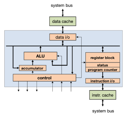
Instruction Set Architecture (ISA) is the interface between a computer’s software and hardware, which defines the set of instructions that a computer’s processor can execute. It specifies the types of instructions that can be used and the format of those instructions, as well as the memory and input/output operations that can be performed by the processor.
We can differentiate the processors by their instruction complexity (e.g. RISC or CISC), type of instruction-level parallelism (dynamically scheduled superscalars or statically scheduled VLIW) as well as by application-specific areas of their employment. The performance of processors can be significantly improved by exploiting instruction-level parallelism (ILP).
The high-level code is transformed by a compiler into an ISA-specific machine code (also called binary or object code). Alternatively, the target code can be written in an assembly language by specifying the program functionality using target ISA instructions.
On the hardware side, the actual processor decodes instructions and generates control signals that are necessary for instructions’ execution. The control signal specification is ISA and processor-dependent.
An Instruction Set Architecture (ISA) typically includes several key parameters that define the capabilities and functionality of a processor. These parameters can include: (1) Data Types: types of data that the processor can handle, such as integers, floating-point numbers, and memory addresses. (2) Instructions: the set of instructions that the processor can execute, such as arithmetic and logic operations, branching, and memory access. (3) Registers: the number and size of registers that the processor has, which are used to temporarily store data and perform calculations. (4) Memory Models: the memory models that the processor supports, such as a flat or segmented memory model, and how memory is accessed and managed by the processor.
For example, the MIPS instruction set consists of different instruction groups. Arithmetic instructions perform arithmetic operations on the registers, e.g. addition and subtraction. Load/store instructions read and write data from the registers to the main memory. Jumps and branch instructions change the sequential execution flow of the target program. They are used to construct loops or when the program execution must be conditioned.
The register file consists of a fixed number of architecture registers. The ISA specifies how the corresponding registers can be used and what kind of information they contain at a certain moment of execution.
The accessible memory region is defined by the address space.
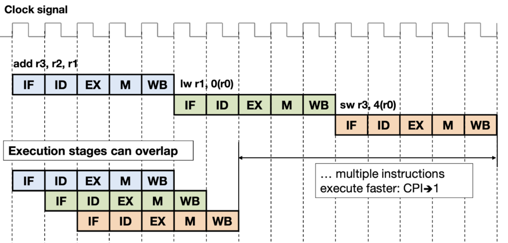
A program is executed in the following sequence: • Instruction fetch (IF): The program counter is incremented and the next instruction is fetched into instruction register (IR). If the instruction was present in the instruction cache, IF takes only 1 clock cycle; otherwise the instruction must be loaded from the main memory, taking more cycles. • Instruction decode (ID): The processor decodes the instruction in IR, and a set of control signals is generated. Then the processor retrieves the operands from registers specified in the instruction. • Execution (EX): In this stage, computational instructions are executed in the ALU and their result is stored in the accumulator. For load/store instructions, the effective memory address is calculated. • Memory (MEM): If the current instruction is load/store, the content of a register in the register block is read from or written to the main memory. • Write back (WB): The result of computational instructions or the data retrieved by load instructions is written back into the register block.
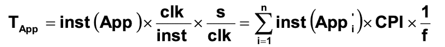
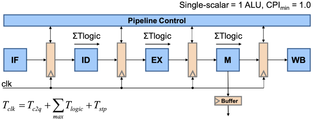
To enable pipelining in hardware, the result of each pipeline operation has to be stored in the intermediate registers at each clock cycle. The period of the clock signal (or its maximum frequency) is defined by the longest pipeline stage. The total instruction rate is typically expressed in MIPS (Millions of Instructions Per Second) and can be determined by dividing the clock frequency of a processor by its CPI value (f / CPI).
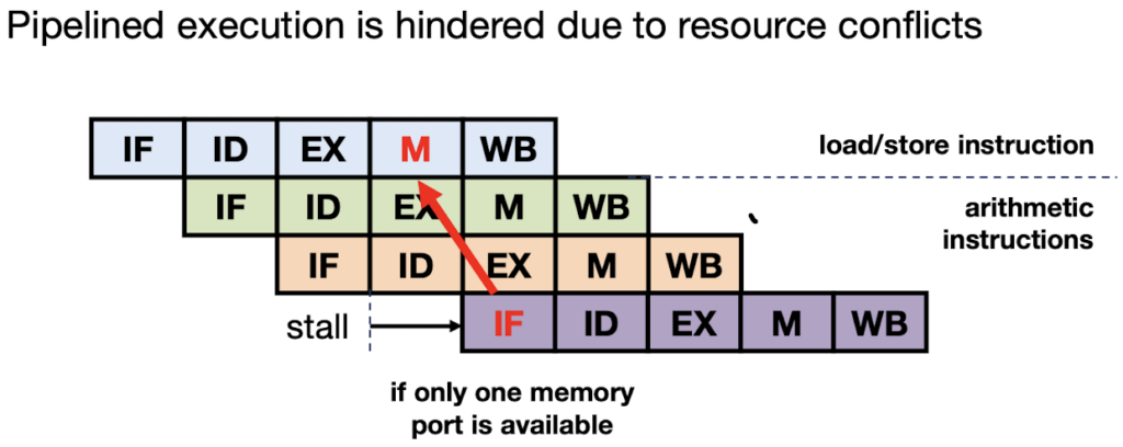
StructuralHazards: Structural hazards occur if a resource conflict exists between instructions in the pipeline. Assume that the processor has only one memory port that is used both for fetching instructions and data load/store operations, then IF and MEM cannot be done in one cycle.
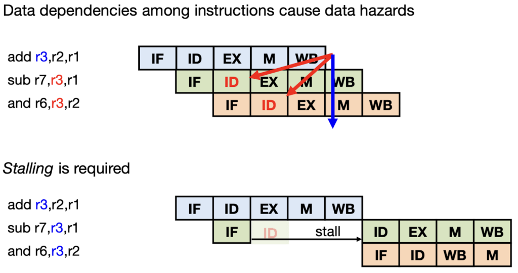
Data Hazards: In a pipeline, a data hazard arises if a result of an operation is required before it has been calculated.
The pipeline has to be stalled until the first instruction writes the right value into register r3.
Control Hazards: If a branch operation causes the program counter to jump to another location, the instructions in the pipeline following the branch have to be flushed and the pipeline has to be filled again starting from the correct instruction.
The overall performance loss due to control hazards is typically even greater than the loss due to data hazards. To cope with this, current processors employ branch prediction in order to predict the right instruction after branches.
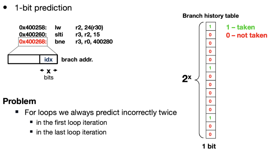
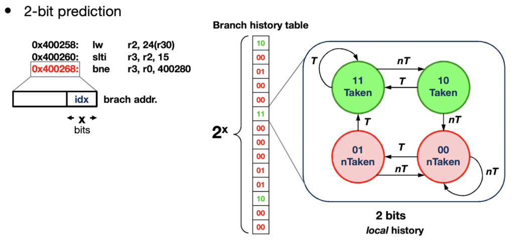
Branch History Table(BHT):
In a 1-bit branch predictor, we assume that the next outcome of a branch is likely to be the same as the previous outcome stored in the table. The last outcome of a branch (taken or not taken) is stored in a 1-bit branch history table. The table is indexed by the last x bits of the branch address, and, thus, the branch table contains 2x elements in total. In loops, the 1-bit branch predictor always predicts incorrectlytwice: after the first loop iteration (because the branch was not taken before), and at the last loop iteration when we exit the loop (because the branch was previously taken).
Branch accuracy can be further improved using 2-bit branch prediction, where two bits are used to encode the state of each branch in the branch history table. A branch will be predicted as taken only if it has been previously taken two times in a row. The same is valid for the branch to be considered as non-taken.
In general, by observing m last outcomes of former branches, we will get 2m possible branch predictors for each branch in the history table. In general, we can define an (m, n)-predictor in which the last m branches are analyzed to select one of the 2m n-bit predictors for the current branch.
A superscalar processor uses multiple execution units within the processor, each of which can execute a different instruction at the same time. To effectively utilize the multiple execution units in a superscalar processor, the processor must be able to identify independent instructions that can be executed concurrently. This is typically done using a combination of static analysis (analyzing the code at compile time) and dynamic analysis (analyzing the code as it is being executed).
Very Long Instruction Word (VLIW) processors use multiple execution units to improve performance by taking advantage of instruction-level parallelism (ILP) in a program, like superscalar processors.
One key difference between VLIW processors and superscalar processors is that VLIW processors rely on static analysis (analyzing the code at compile time) to identify independent instructions that can be executed concurrently, while superscalar processors also use dynamic analysis (analyzing the code as it is being executed). This means that VLIW processors must be specifically designed and optimized for the types of programs they will be running, while superscalar processors can adapt to a wider range of programs.
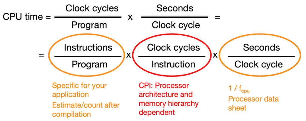
There are several ways to measure the performance of a CPU, ultimately we are interested in CPU time of a program, task or function.
Cycles per instruction (CPI) is a measure of the number of clock cycles that a CPU requires to execute a single instruction. It is used to evaluate the performance of a CPU and to compare the performance of different processors.
A lower CPI indicates that a CPU can execute instructions more quickly and efficiently. Factors that can affect CPI include the complexity of the instruction set, the number of clock cycles required to execute each instruction, and the amount of time required to access data from memory.
It is important to note that CPI alone does not reflect the overall performance of a CPU. A high clock speed or a high number of instructions per clock (IPC) can offset a high CPI, and other factors such as cache size and memory bandwidth can also affect overall performance. Thus it’s used in conjunction with other metrics to get a complete picture of a CPU’s performance.
We can decompose CPIMEM into CPI of instruction accesses and CPI of data accesses. In a system with cache memory, if data/instructions are in the cache, the access time is 1 cycle, otherwise, there is a penalty (i.e. an increased number of cycles).
In a cache, an address is divided into three parts: offset, index, and tag.
Offset: The offset is the least significant bits of the address, and it is used to identify a specific byte within a cache line. The size of the offset depends on the size of the cache line. For example, if the cache line size is 64 bytes, the offset would be 6 bits (2^6=64).
Index: The index is the next most significant bits of the address, and it is used to identify a specific cache line within the cache. The size of the index depends on the number of cache lines in the cache. For example, if the cache has 64 lines, the index would be 6 bits (2^6=64).
Tag: The tag is the most significant bits of the address, and it is used to identify a specific block of memory within main memory. The tag is used to compare the memory address being accessed to the addresses stored in the cache. If the tag matches, then the data is likely to be in the cache, and the index and offset are used to locate it.
Direct-mapped cache: The cache is divided into a fixed number of lines, and each line has a unique address. Each block of main memory is mapped to a specific location in the cache.
Set-associative cache: The cache is divided into a fixed number of sets, and each set contains a fixed number of lines. Each block of main memory can be mapped to one of several locations in the cache.
Fully associative cache: In this type of cache organization, each block of main memory can be mapped to any location in the cache. The cache is not divided into sets, and each block of memory is compared to all the tags in the cache. To determine if a block of memory is in the cache, the address is divided into two parts: the offset and the tag. The tag is used to identify a specific block of memory, and the offset is used to identify a specific byte within a cache line.
In the set-associative cache, when a cache line set is full and a new block of memory needs to be added, one cache line will be replaced. The most commonly used cache replacement policies are:
Least Recently Used (LRU): This policy replaces the cache line that has not been accessed for the longest period of time. It works by maintaining a linked list of the cache lines in order of the time they were last accessed, with the most recently accessed line at the front of the list and the least recently accessed line at the back of the list. When a new block of memory needs to be added to the cache, the least recently accessed line is removed from the list and replaced with the new data.
Least Frequently Used (LFU): This policy replaces the cache line that has been accessed the least number of times. It works by maintaining a counter for each cache line that keeps track of how many times the line has been accessed. When a new block of memory needs to be added to the cache, the line with the lowest access count is removed from the cache and replaced with the new data.
First In First Out (FIFO): This policy replaces the oldest block in the cache. It works by maintaining a queue of the cache lines in the order they were added, with the oldest block at the head of the queue and the newest block at the tail of the queue. When a new block of memory needs to be added to the cache, the oldest block is removed from the queue and replaced with the new data.
Random: This policy replaces a random block in the cache. It works by randomly selecting a cache line to be replaced when a new block of memory needs to be added to the cache.
Cache write strategies determine how data is written to the cache when a block of memory is updated or modified. Some common cache write strategies are:
Write-Through: In this strategy, data is written to both the cache and the main memory at the same time. This ensures that the data in the cache is always consistent with the data in the main memory. However, this strategy can result in increased write traffic to the main memory, which can slow down the system.
Write-Back: In this strategy, data is first written to the cache, and then written to the main memory at a later time. This can improve system performance by reducing the number of writes to the main memory. However, it also increases the chances of cache data becoming inconsistent with main memory data in case of system crashes or power failures.
In a write-back cache, a “dirty bit” is used to keep track of whether a block of memory in the cache has been modified (written to) or not.
When a block of memory is first brought into the cache, the dirty bit is set to “not dirty” (or “clean”). If a write operation is then performed on the block of memory in the cache, the dirty bit is set to “dirty” to indicate that the block of memory has been modified and the copy in the main memory is no longer up-to-date.
When the cache replacement algorithm decides that a dirty block needs to be evicted, the data in that block is written back to main memory first, so as to maintain the consistency between the main memory and the cache.
The use of dirty bits allows the write-back cache to avoid writing back all blocks to main memory, thus reducing the number of writes to main memory and improving performance.
We first clarify some basic definitions in the context of memory:
Access bandwidth [bits/s]: Amount of data transported into or out of a memory array (or memory interface) per unit of time.
Latency: Delay or time elapsed between the request and actual delivery of data.
Cycle time: Minimum time period between two consecutive read or write accesses to memory.
Asynchronous memory, also known as asynchronous DRAM, does not operate in sync with the clock speed of the computer’s processor. Instead, it operates on its own clock, which can be slower or faster than the processor’s clock. This results in longer access times, but it also means that asynchronous memory can be manufactured using simpler and less expensive technology.
Synchronous memory operates in sync with the clock speed of the computer’s processor. This results in faster access times, as the memory and processor can work in tandem to quickly transfer data. However, synchronous memory is typically more expensive to manufacture, as it requires more advanced technology to synchronize its operation with the processor’s clock.
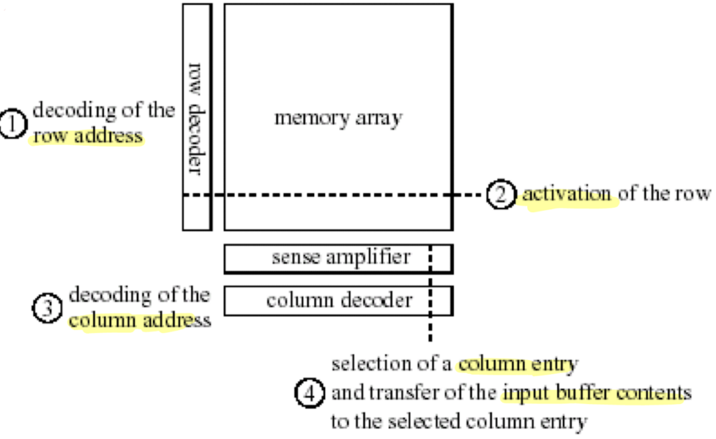
Burst access modes allow for reading/writing more than a single data word from/to memory. In order to store/retrieve larger chunks of information to/from consecutive memory locations, it is sufficient to increment the column decoder address lines (while keeping the row decoder lines fixed). The maximum burst size (i.e. number of words that can be accessed during one burst command) equals the number of words in one word line (= 2K).
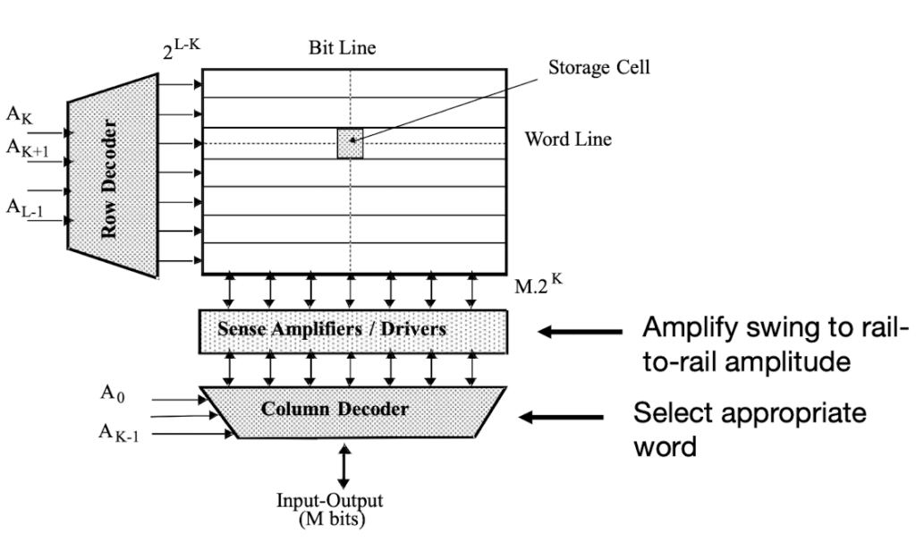
Hierarchical Memory Architecture An assembly consisting of a memory cell matrix, a row decoder, and a column decoder is a memory block or page. Memory blocks can be cascaded horizontally, further partitioning the address bits into block address, column address, and row addresses.
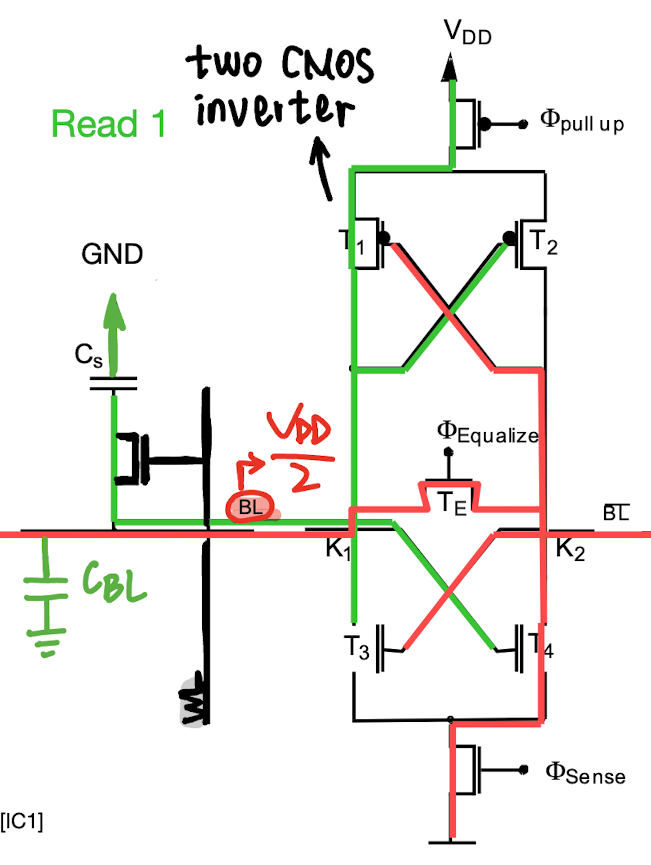
The transistor acts as a switch which is controlled by the word line WL. The bit information is stored in the storage capacitor CS. BL is precharged to VDD/2.
When a logic “1” (VDD) shall be written to a particular memory cell, the corresponding BL and WL lines are driven with VDD. As a consequence, CS is charged to “1”, i.e., VDD-Vt (If there was already a “1” stored on CS, the logic level is refreshed.) Similarly, storing a “0” is realized by driving BL to GND which discharges CS.
When a particular memory cell is read, the corresponding BL and WL lines are driven with VDD. In case a “1” was stored, the voltage of CS is VDD-Vt, which is greater than the voltage of CBL: VDD/2, the charge redistribution between CS and the bit line capacitor CBL raises the voltage on BL. As CS is much smaller than CBL, the total charge Q = QS+QBL = CSVS + CBLVBL keeps unchanged, this voltage swing is small compared to VDD. However, it’s big enough to be sensed by the sense amplifier who drives BL to VDD and recharges CS. Hence, during a DRAM read, the stored “1” of the memory cell is re-written.
CS may lose the stored content due to charge leakage. That’s why the stored content in DynamicRAM memories has to be refreshed periodically when the time between consecutive memory accesses exceeds certain intervals.
Trench DRAM Cell implements the conducting electrodes of the capacitor along the walls of a deep and narrow trench cut into the Si substrate, which increases the storage capacity CS, thus the information stored is more robust.
Activation of the word line WL connects the storage capacitor CS to BL. If CS was charged to VDD (Reading a “1”), the voltage on BL will slightly increase, which makes T4 conduct and the voltage on T1 decrease. Thus, T1 conducts, BL is connected to VDD and the originally stored logic level on CS is refreshed.
In DRAM, a sense amplifier is not necessary, but we use it for performance reasons.
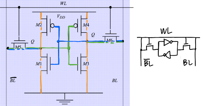
In contrast to the 1 transistor DRAM cell, the SRAM cell needs no periodic refreshing and keeps the stored bit value unless it is disconnected from the power supply.
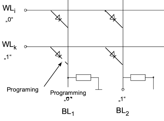
An open fuse represents a logic “0”, whereas a closed fuse represents a logic “1”.
The diode prevents reverse currents to flow from BL to WL and, thus, impacting the logic values on other BL. The resistor between the BL and GND is mandatory to discharge CBL after each access, thus ensuring a proper “0” level.
When programming the floating gate transistor cell, a high programming voltage (e.g. four times higher than VDD) is applied to both the control gate and the drain (bit line), making electrons able to tunnel through the first oxide layer onto the floating gate. Removing the programming voltages leaves negative charge trapped on the floating gate. When now applying VDD to the control gate (word line) the effective floating gate to substrate voltage isn’t large enough to establish a conducting channel. The negative voltage on the floating gate results in a higher threshold voltage Vt.
In contrast to EPROM, EEPROM, and flash memory cells are electrically erasable. Erasing a stored bit value means removing the trapped charges from the floating gate. This can be done by making the source electrode float (disconnect from GND), connecting the drain electrode to a high voltage, and the control gate to GND. Thus, electrons on the floating gate are attracted through the thin oxide layer to drain. This effect is called “Fowler-Nordheim” tunneling.
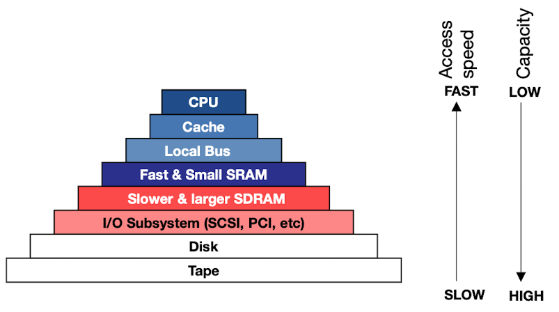
CPU caches are closely integrated with the processor core and operate at the same cycle times as the CPU data path pipelines.
The next faster (and bigger) data repository is on-chip (or off-chip) SRAM. However, in order to access SRAM, the CPU request already has to traverse across the CPU bus introducing additional latency.
For larger quantities of data, external SDRAM (or variants) are the next choice. The single transistor DRAM cell achieves larger storage densities than the six transistor SRAM cell, but introduces longer access times due to the more complex access mechanism and the need to interleave data accesses with periodic refresh cycles.
SDRAM memory acts as a “mirror space” for data residing on the hard disk. DMA (direct memory access) controllers shuffle data from external disk drives via system interfaces (e.g. PCI, SCSI) into the SDRAM without requiring CPU attention.
The memory controller translates the linear addresses for read and write used by the CPU into two-dimensional (row, column) addresses and corresponding control signals for SDRAM internal use. In general, memory controllers hide features and requirements of a specific memory technology. If necessary, the memory controller can stall the CPU until the SDRAM is again able to accept subsequent read or write accesses. Three buses are distinguished for data (b), control signals (c), and addresses (a). In some systems, combinations of these signals are multiplexed onto a single bus.
.
.
. In order to obtain higher speed circuits, capacitive load
.
.


.